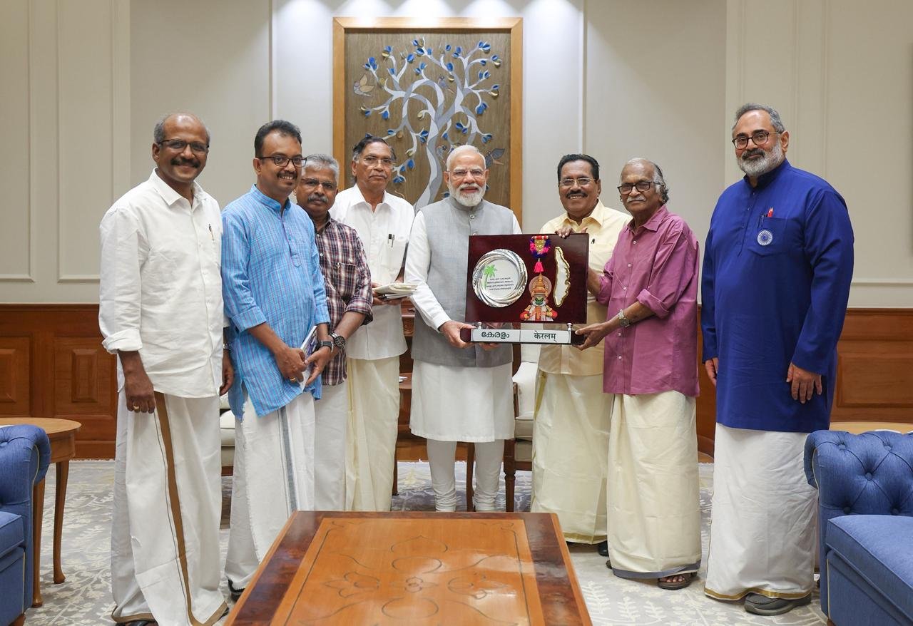
 During the visit, 28 student-designed semiconductor chips from 17 academic institutions were handed over. These chips were developed using Electronic Design Automation (EDA) tools under the Chips to Start-up (C2S) program, bringing the total fabricated student-designed chips at SCL to 56. Shri Vaishnaw emphasised that SCL will continue to support students, researchers, and start-ups by turning their designs into real silicon.
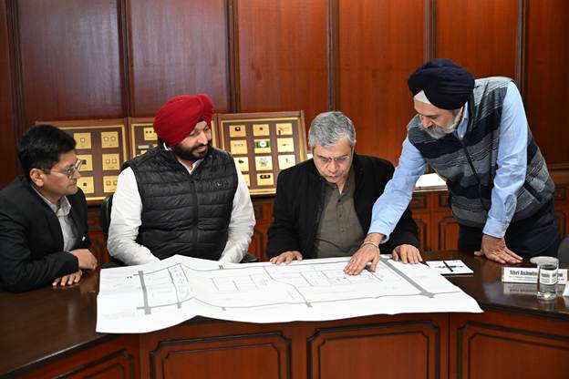
The Minister inaugurated the Semiconductor Process Gallery and the Abhyuthanam Training Block. The Process Gallery provides students with hands-on experience of a clean room lab and ATMP facility, while the Training Block offers both online and offline semiconductor modules along with fire and safety training.
Shri Vaishnaw highlighted the roadmap for SCL Mohali under Prime Minister Narendra Modi’s vision, which includes a significant increase in production capacity, targeting a 100-fold rise in wafer production. The government has requested 25 acres from the Punjab Government to support this modernisation drive.
India is among the few countries where nearly 300 universities participate in designing semiconductor chips using world-class EDA tools provided by government initiatives. Shri Vaishnaw underlined that SCL will remain a platform for talent development, innovation, and start-up growth.
Emphasising Atmanirbharta in strategic sectors, he stated that India will build a robust ecosystem for indigenous chip development. A consortium comprising CDAC, DRDO, and other organisations will collaborate on the design, product development, and manufacturing of Swadeshi chips.