
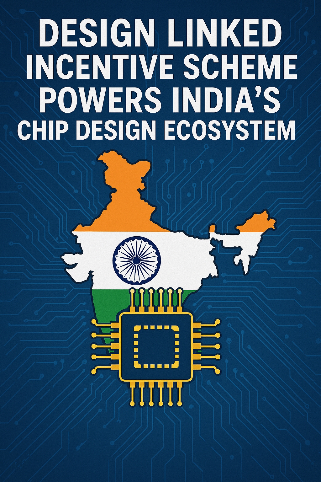
 Why Chip Design Matters Most
Globally, semiconductor chip design accounts for up to 50 percent of total value addition, nearly half of the bill of materials cost, and over one-third of total industry sales through the fabless model. Unlike manufacturing-heavy fabs, chip design delivers high economic value with relatively modest capital investment.
Without strong domestic design and intellectual property ownership, even countries with electronics manufacturing capacity remain dependent on imported core technologies. The DLI Scheme directly addresses this gap by nurturing India’s fabless ecosystem and enabling long-term control over critical technologies.
What the DLI Scheme Offers
Implemented by the Ministry of Electronics and Information Technology (MeitY) through the India Semiconductor Mission, the DLI Scheme provides financial incentives and shared design infrastructure to eligible startups, MSMEs and domestic companies. It supports the full lifecycle of semiconductor products, including integrated circuits, chipsets, systems-on-chip, systems and IP cores.
Under the Product Design Linked Incentive, companies can receive reimbursement of up to 50 percent of eligible expenditure, capped at ₹15 crore per application. The Deployment Linked Incentive offers 6 to 4 percent of net sales turnover for five years, with a maximum cap of ₹30 crore, provided the designed chip is successfully deployed in electronic products.
World-Class Design Infrastructure
A major strength of the DLI Scheme is access to national-scale design infrastructure through the ChipIN Centre established by C-DAC. This includes a centralized grid of advanced Electronic Design Automation tools, IP core repositories, multi-project wafer prototyping support and post-silicon validation facilities.
The shared EDA Grid has emerged as one of the largest centralized chip design platforms in the world, supporting nearly one lakh engineers and students across 400 institutions. As of January 2026, supported startups alone have logged over 54 lakh hours of EDA tool usage, reflecting deep ecosystem adoption.
Tangible Outcomes on the Ground
Since its launch in December 2021, the DLI Scheme has delivered measurable results. Twenty-four chip design projects have been sanctioned across strategic domains such as video surveillance, drone detection, smart energy metering, microprocessors, satellite communications and IoT systems-on-chip.
Six semiconductor chips have already been fabricated, 16 design tape-outs completed and ten patents filed. More than 1,000 specialised engineers are currently engaged in DLI-supported projects, while over 140 reusable semiconductor IP cores have been developed, strengthening India’s design foundation.
Indian Startups Leading the Way
Several DLI beneficiaries have emerged as flagbearers of India’s semiconductor design ambitions. Companies like Vervesemi Microelectronics are building motor-control chips for consumer appliances and electric mobility, while InCore Semiconductors is advancing indigenous RISC-V microprocessor IPs for embedded and edge-AI applications.
Netrasemi has achieved a milestone by taping out India’s first indigenously designed AI SoC at an advanced 12 nm node, while Aheesa Digital Innovations and AAGYAVISION are delivering solutions in broadband connectivity and radar-on-chip technologies. These successes highlight India’s growing credibility in global chip innovation.
Institutional Backbone
The DLI Scheme operates within a broader institutional framework led by MeitY and the ₹76,000-crore Semicon India Programme. Complementary initiatives such as the Chips to Startup Programme and the Microprocessor Development Programme are building skilled manpower and open-source processor architectures.
Together, these efforts bridge the gap between academic research, startup innovation and commercial deployment, ensuring that chip design excellence translates into market-ready products.
Strategic Impact
As DLI-supported designs move toward volume manufacturing and system integration, India is positioning itself as a reliable partner in the global semiconductor value chain. The scheme reduces import dependence, enhances supply-chain resilience and ensures access to critical technologies for defence, telecom, artificial intelligence and mobility.
More importantly, it anchors India in the most strategic layer of the semiconductor ecosystem design and intellectual property laying the foundation for sustainable economic growth and technological sovereignty.