


The project, to be developed by India Chip Pvt. Ltd., marks a significant step in strengthening India’s semiconductor manufacturing ecosystem. It reflects the government’s broader push toward technological self-reliance and high-end electronics production.
The facility will function as an Outsourced Semiconductor Assembly and Test (OSAT) unit under the Modified Scheme for Semiconductor Assembly, Testing, Marking and Packaging (ATMP). The total investment in the project is estimated to exceed ₹3,700 crore.
Boost to Domestic Manufacturing
The upcoming semiconductor plant is aligned with the Centre’s efforts to reduce import dependence and build resilient global supply chains. By establishing advanced chip assembly and testing capabilities domestically, the project aims to strengthen India’s manufacturing base.
The facility is expected to support multiple high-growth sectors, including mobile phones, tablets, laptops, automotive electronics and consumer devices. With rising demand for semiconductor components, the plant will play a critical role in meeting domestic needs.
Industry observers believe that the HCL–Foxconn partnership underlines India’s emergence as a trusted global destination for electronics manufacturing.
Employment and Ancillary Growth
Beyond manufacturing capacity, the semiconductor unit is expected to generate thousands of direct and indirect employment opportunities. Engineers, technicians and skilled professionals are likely to benefit from the project.
Additionally, the facility is expected to catalyse growth in ancillary industries, including packaging materials, testing equipment and logistics services. This multiplier effect could significantly enhance the regional industrial ecosystem around YEIDA.
Strategic Importance for India
The HCL–Foxconn joint venture highlights India’s growing stature in the global semiconductor landscape. As nations worldwide compete to secure chip supply chains, India’s push into advanced semiconductor assembly and testing signals long-term strategic intent.
The project also aligns with broader government initiatives aimed at fostering innovation, skill development and technology transfer within the country.
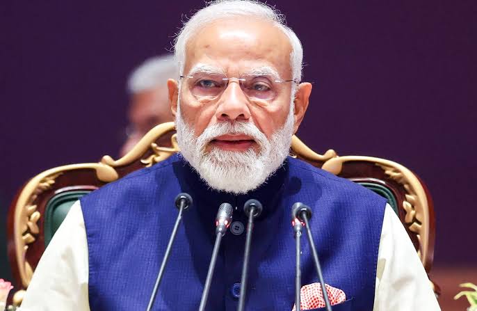
With the groundbreaking ceremony, India moves closer to building a robust and self-reliant electronics manufacturing ecosystem. The participation of the Prime Minister underscores the strategic priority attached to semiconductor development in the country’s economic roadmap.