
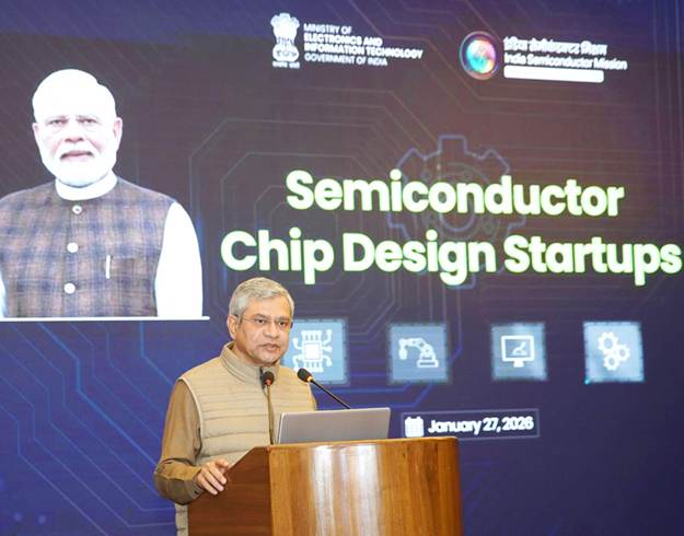

Minister Vaishnaw emphasised that the government aims to enable at least 50 fabless semiconductor companies in the next phase of the programme. Currently, 24 startups have achieved significant milestones, including tape-outs, validated products, and market traction. The programme has also resulted in 75 patents filed by academic institutions and 10 by startups, bolstering India’s indigenous IP portfolio.
Highlighting global recognition, the Minister noted that international stakeholders, initially sceptical in 2022, now see India as a serious and capable player in the semiconductor ecosystem. This shift in perception has attracted venture capital investment of nearly ₹430 crore, with 14 of the 24 DLI startups securing funding.
Focus Areas and Strategic Sectors
The government outlined six strategic domains for semiconductor design: compute systems, RF and wireless, networking, power management, sensors, and memory. These focus areas form the foundation for applications across defence, space, automotive, drones, and critical infrastructure.
Infrastructure support includes SCL Mohali for 180-nm tape-outs and the upcoming fabrication facility at Dholera enabling advanced nodes up to 28 nm. These developments complement the domestic design ecosystem and enhance India’s capability to design and manufacture chips for nearly 70–75% of domestic applications by 2029.
Talent Development and Deep Tech Awards
Minister Vaishnaw underscored talent development as a core pillar, with over 67,000 semiconductor professionals trained in four years against a 10-year target of 85,000. To further foster innovation, the government will institute Deep Tech Awards in 2026 to recognise breakthroughs across semiconductors, AI, biotechnology, space, and other advanced technology sectors.
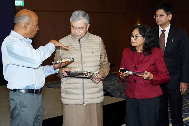
The interaction also provided a platform for startups to showcase their tape-out milestones and commercialization strategies, highlighting the importance of indigenisation and trusted domestic supply chains. Secretary, MeitY Shri S. Krishnan, and CEO, ISM Shri Amitesh Kumar Sinha were also present during the event.
With strategic infrastructure, global engagement, and focus on six critical semiconductor design domains, India is on course to establish itself as a leading global hub for chip design and manufacturing.